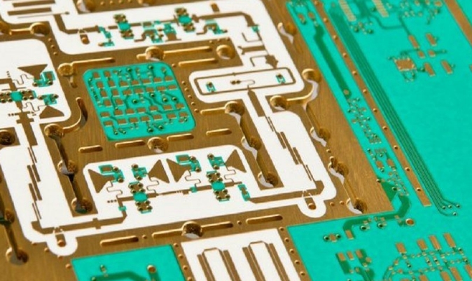
High-frequency PCB design requires careful consideration of various factors to ensure signal integrity, minimize electromagnetic interference (EMI), and achieve optimal performance. In this comprehensive guide, we will explore the key guidelines and best practices for designing high-frequency PCBs.

1.Material Selection:
Choose a low-loss dielectric material with a high relative permittivity (εr) to minimize signal losses and improve signal integrity. Common materials include FR-4, PTFE (Teflon), and Rogers materials.
Consider the dissipation factor (loss tangent) of the material, as it affects the signal attenuation and phase distortion at high frequencies.
2.Layer Stackup:
Implement a balanced stackup with controlled impedance to maintain signal integrity and minimize crosstalk.
Use a solid ground plane as the reference plane for signal layers to provide low impedance return paths and reduce EMI.
Avoid layer transitions beneath high-speed signals to prevent impedance mismatches.
3.Transmission Line Design:
Use controlled impedance traces to match the characteristic impedance of the transmission lines. This minimizes signal reflections and ensures efficient signal transfer.
Calculate the required trace width and spacing based on the dielectric constant, trace thickness, and desired impedance using impedance calculators or design software.
Differential pair routing should maintain consistent spacing and parallelism to preserve signal balance and minimize crosstalk.
4.Via Design:
Minimize the number of vias in high-frequency paths to reduce signal distortion and improve signal integrity.
Use via stitching to provide a low impedance path for return currents and reduce the ground loop area.
Consider using blind or buried vias for layer transitions to minimize signal reflections.
5.Decoupling and Power Distribution:
Place decoupling capacitors near high-speed ICs to provide a low-impedance path for high-frequency current demands.
Use a combination of low-ESR (Equivalent Series Resistance) and high-capacitance capacitors to filter out high-frequency noise.
Create a solid power and ground plane for effective power distribution and to minimize voltage drops and EMI.
6.EMI/EMC Considerations:
Minimize loop areas by routing high-speed traces adjacent to the ground plane.
Apply proper shielding techniques, such as using grounded copper pours or shielding cans, to reduce electromagnetic radiation and susceptibility.
Implement signal filtering techniques like ferrite beads, common-mode chokes, and shielding to reduce EMI emissions and susceptibility.
7.Thermal Management:
High-frequency PCBs can generate heat, so consider thermal management techniques like heat sinks, thermal vias, and copper pours to dissipate heat effectively.
Optimize component placement to allow for proper airflow and heat dissipation.
8.Design for Manufacturing (DFM):
Follow manufacturing guidelines for the selected PCB fabrication process, such as minimum trace widths and spacing, minimum annular rings, and solder mask clearances.
Communicate with your PCB manufacturer to ensure they can meet your design requirements for impedance control and tolerances.
9.Simulations and Prototyping:
Utilize simulation tools, such as electromagnetic field solvers, to analyze and optimize high-frequency signal behavior, impedance matching, and EMI/EMC performance.
Build and test prototypes to validate the design and fine-tune parameters if necessary.
10.Signal Integrity Analysis:
Perform signal integrity analysis, such as eye diagram analysis, return loss analysis, and time-domain reflectometry (TDR), to verify the high-frequency performance of the PCB design.
Remember that high-frequency PCB design is a complex field, and these guidelines provide a starting point. It's essential to stay updated with the latest technologies, tools and industry standards.

Overcoming Hurdles in High Frequency PCB Design
Designing high-frequency PCBAs shares common principles with other board designs, following IPC standards for reliability and manufacturability. However, the challenges intensify when dealing with high-frequency boards, necessitating additional considerations to meet stringent performance criteria. Some of these challenges are highlighted below.
Radiation Management: High-frequency and high-speed boards often incorporate components emitting electromagnetic interference (EMI). Devices like wireless transmitters, converters, and power supplies can generate onboard EMI, impacting the electromagnetic compatibility (EMC) of the environment where the board is deployed.
Absorption Sensitivity: Conversely, the board may be susceptible to absorbing radiation from neighboring boards or devices, potentially affecting its performance.
Signal Integrity: Preserving signal integrity is crucial, addressing issues such as mismatched differential pairs, excessive transmission line lengths, inadequate shielding, or other factors contributing to signal degradation.
Reflection Mitigation: Impedance matching is vital to preventing reflections that can compromise signal integrity, redirecting signals back toward the source instead of transmitting them.
Coupling Challenges: Proximity between two conductors can lead to coupling issues, adversely affecting signal propagation. Careful spacing is crucial in the PCB layout design to minimize these effects.
Parasitic Capacitance: Unwanted coupling often stems from parasitic capacitance. Although it cannot be entirely eliminated, its effects can be minimized through careful design considerations.
Harmonic Distortion Management: Harmonic distortion poses a common threat to signal integrity. Frequency shifts can manifest as issues, particularly in TX/RX systems.
Common Mode Noise: Boards featuring power supplies or conversion circuitry may encounter common mode noise due to stray capacitance between terminals.
Surface Tracking Concerns: For high-voltage and/or current PCBAs, surface tracking—degraded insulation creating a current path—can pose dangers, potentially leading to burned components or fires.
While the challenges listed above are not exhaustive, they underscore the need for meticulous care in high-frequency PCB designs. Addressing these concerns ensures the reliability and optimal performance of electronic systems operating at elevated frequencies.
Get more knowledge about High Frequency PCB Design Guidelines please refer to Rigaopcb:https://www.rigaopcb.com/