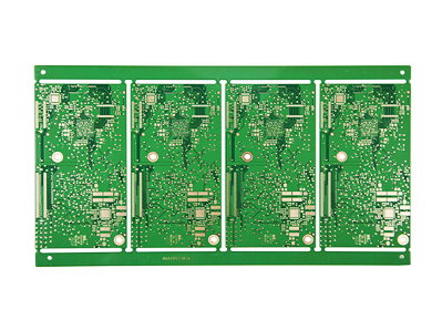
HDI PCBs are a type of advanced printed circuit boards that are designed to have higher trace density, smaller vias, and finer line widths and spacing. These boards are used in applications where space is limited, and there is a need to achieve higher circuit density and performance.

The HDI standard in PCB design encompasses several key features and technologies:
1.Microvias: HDI PCBs use microvias, which are small vias with diameters typically less than 150 micrometers. Microvias allow for increased routing density and enable the connection of multiple layers in a compact space.
2.Blind Vias: Blind vias are vias that connect an outer layer of the PCB to one or more inner layers but do not penetrate through the entire board. They allow for shorter signal paths and more efficient use of available space.
3.Buried Vias: Buried vias are vias that connect multiple inner layers of the PCB without extending to the outer layers. Buried vias further increase routing density and help reduce signal interference.
4.Fine Traces and Spacing: HDI PCBs use fine traces and spacing, typically with line widths and spaces below 100 micrometers. This enables more complex circuits and miniaturization.
Stacked Microvias: Stacked microvias are multiple microvias stacked on top of each other, providing more routing channels for high-density designs.
HDI PCBs are commonly used in modern electronics such as smartphones, tablets, laptops, and other compact electronic devices. They allow for efficient use of space, improved signal integrity, and better performance compared to traditional PCBs.
The specific HDI standard and design rules can vary based on the requirements of the application and the capabilities of the PCB manufacturing process used. Designers and manufacturers follow specific guidelines and rules to ensure the successful fabrication of HDI PCBs with high reliability and performance.
Get more knowledge about What is the HDI standard in PCB please refer to Rigaopcb:https://www.rigaopcb.com/