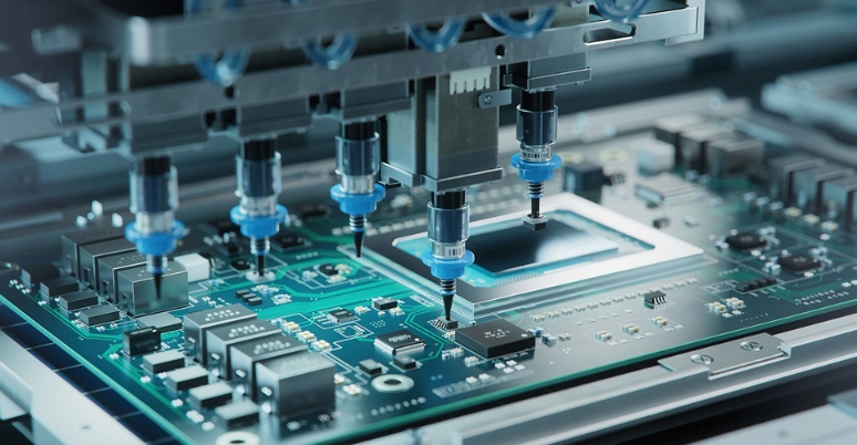
In the world of electronics manufacturing, the printed circuit board (PCB) assembly process is akin to the heart of the operation. Getting it right is crucial. That's where inspection swoops in – it's the unsung hero ensuring everything's in tip-top shape. Imagine setting off on a road trip without checking your car; that's what skipping inspection is like – a potential journey to failure town.

Why bother with scrutinizing things in detail?The answer is straightforward. It boils down to the importance of stopping small mistakes from snowballing into huge catastrophes.
If checks aren't thorough, a bad circuit board might slip through without being spotted, causing problems for the device it controls.
This stage of checking is crucial in guaranteeing the dependability, effectiveness, and durability of the product."
Visual Inspection, or VI, is the Sherlock Holmes of inspection methods. It's all about scrutinizing the PCB with the naked eye or a magnifying tool. Inspectors look for obvious issues – think soldering defects, missing components, and alignment issues.
VI is economical and straightforward but has its kryptonite – human error. It’s excellent for catching glaring issues but might miss subtler defects.
Picture this: a high-speed camera zipping above a PCB, capturing meticulous details. That's AOI in a nutshell. It uses sophisticated software to compare the captured images against a perfect prototype.
AOI is like having Superman's vision; it spots defects faster and more reliably than human eyes, making it a staple in large-scale production.
AOI shines brightest when used after soldering to catch any solder defects or component placement issues early on.
X-Ray inspection is the superhero with X-ray vision. It can see through components, uncovering hidden issues like solder bridges or voids that AOI might miss.
This method is a game-changer for inspecting multi-layer boards or complex packages like BGAs (Ball Grid Arrays), where visual inspection methods hit a wall.
In-Circuit Testing is like giving the PCB a physical exam. It involves testing each component systematically to ensure it functions correctly within the circuit.
ICT is thorough but comes with a drawback – it requires custom fixtures, making it less adaptable and more expensive.
This is the final frontier, where the PCB is powered up and taken for a spin to see if it performs as expected in a real-world scenario.
Functional testing ensures that the PCB not just looks good but also does its job, providing the ultimate peace of mind before it heads out into the world.
Selecting an inspection method is about balancing needs and resources. It's crucial to weigh the complexity of the PCB, the volume of production, and the acceptable risk level. Often, a combination of methods is the key to covering all bases.
PCB inspection methods are the unsung heroes in electronics manufacturing, each with its unique strengths. Whether it's the meticulous eye of VI or the high-tech prowess of AOI and X-Ray, inspection ensures that only the best PCBs make it through the gates. Remember, the goal is always quality, reliability, and functionality.
1. Can visual inspection alone suffice for PCB inspection?
While VI can capture obvious defects, it's often complemented with other methods like AOI for a more thorough inspection.
2. How does AOI differ from X-ray inspection?
AOI relies on optical images and can't see through components, while X-ray inspection offers a deeper look into hidden layers and joints.
3. Is functional testing conducted on each printed circuit board?
Not always. It depends on the project requirements and cost considerations but is highly recommended for complex or critical applications.
4. Why is ICT considered expensive?
ICT needs custom fixtures for each PCB design, increasing the initial setup cost and time.
5. When should X-ray inspection be used in the PCB inspection process?
X-ray inspection is particularly useful for boards with hidden layers or components, such as BGAs, to ensure solder quality and component alignment inside the package.