Creating a Printed Circuit Board (PCB) is a complex and multifaceted process that encompasses both the conceptualization and production stages of the circuit board. This intricate journey begins with the meticulous design of the PCB, a crucial phase where the layout, arrangement of components, and overall specifications are carefully crafted using specialized design software.
Moving beyond the virtual realm of design, the next phase transitions into the tangible realm of manufacturing. This transformative process undergoes a series of sequential steps, each playing a pivotal role in bringing the envisioned PCB to life. From the selection of suitable substrate materials to the precise application of copper cladding onto the board's surface, each step contributes to the formation of the foundational circuitry.
As the fabrication process unfolds, further intricacies emerge, such as the strategic application of photoresist and its subsequent exposure to ultraviolet light. The etching process that follows refines the copper layers, sculpting them into the precise circuit traces dictated by the initial design. Solder mask application then serves to protect and insulate the traces, ensuring the longevity and reliability of the final PCB.
The journey doesn't end with the completion of the circuitry. Silkscreen printing adds informative markings, logos, and reference designators, enhancing the board's functionality and ease of identification. The application of a surface finish acts as a protective layer, guarding the exposed copper from corrosion and oxidation.
The concluding phases of the fabrication process involve rigorous testing procedures to guarantee that the fabricated PCBs not only adhere to the original design specifications but also meet the stringent quality standards expected in electronic manufacturing. This comprehensive and meticulous approach ensures the successful transition from a conceptualized PCB design to a fully functional and reliable circuit board.

Here are the key steps involved in PCB board fabrication:
1. Design: The process begins with the design of the PCB using PCB design software. The design includes the placement of components, routing of traces, and other specifications such as board dimensions and layer stackup.
2. Gerber File Generation: Once the PCB design is complete, Gerber files are generated. Gerber files contain the information needed for manufacturing, including the placement of copper traces, solder mask, and silkscreen.
3. Panelization: In this step, multiple PCB designs are arranged on a panel. This is done to optimize the use of raw materials and improve efficiency during manufacturing.
4. Substrate Material Selection: The choice of substrate material is critical. Common materials include FR-4 (Flame Retardant 4), which is a widely used epoxy-based laminate, and other materials like aluminum or ceramic for specific applications.
5. Cutting and Cleaning Substrate: The substrate material is cut into the desired shape, and any residue or contaminants are cleaned from the surface to ensure good adhesion of the copper layers.
6. Copper Cladding: A thin layer of copper is then added to the substrate. This is typically done through a process called electrodeposition, where copper ions are deposited onto the surface.
7. Photoresist Application: A layer of photoresist is applied to the copper-clad substrate. The photoresist is a light-sensitive material that will be used to transfer the PCB design onto the copper layer.
8. Exposure and Development: The Gerber files are used to create a photomask, which is used to expose the photoresist to ultraviolet light. After exposure, the unexposed photoresist is washed away, leaving the desired pattern on the copper layer.
9. Etching: The exposed copper is then etched away using a chemical process. The remaining copper forms the circuit traces according to the PCB design.
10. Solder Mask Application: A solder mask is applied over the entire surface, leaving openings only where solder pads are required. The solder mask protects the copper traces from oxidation and provides insulation.
11. Silkscreen Printing: Reference designators, logos, and other markings are printed onto the board using a silkscreen layer. This helps in identifying components and provides additional information.
12. Surface Finish: The final step involves applying a surface finish to protect the exposed copper traces. Common surface finishes include HASL (Hot Air Solder Leveling), ENIG (Electroless Nickel Immersion Gold), and OSP (Organic Solderability Preservative).
13. Testing: The fabricated PCBs undergo testing to ensure that they meet the design specifications and that there are no manufacturing defects.
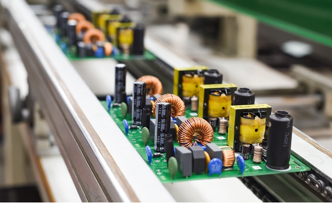
Once the PCBs pass the testing phase, they are ready for assembly, where electronic components are mounted onto the board. The completed assembly can then be integrated into various electronic devices.