Embarking on the journey of PCB development requires a clear understanding of the intricacies involved in the fabrication process. Before delving into the specifics of PCB fabrication, it's essential to explore the relationships between various stages such as PCB development, manufacturing, testing, and assembly.

PCB Development: A Holistic Approach
PCB development encompasses the entire lifecycle of a circuit board design, from conception to production. This iterative process involves three main stages: design, manufacturing, and testing. The goal is to refine and optimize the design for the highest quality within the allotted development time. Each stage contributes to the evolution of the design, ensuring functionality and performance.

PCB Manufacturing: A Two-Step Journey
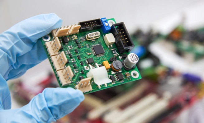
1. Board Fabrication: The manufacturing journey begins with board fabrication, where the designed circuit board layout is imprinted onto copper-clad laminates. Excess copper is then etched from inner layers, revealing traces and pads. The board materials undergo a lamination process at high temperatures to create the PCB layer stackup.
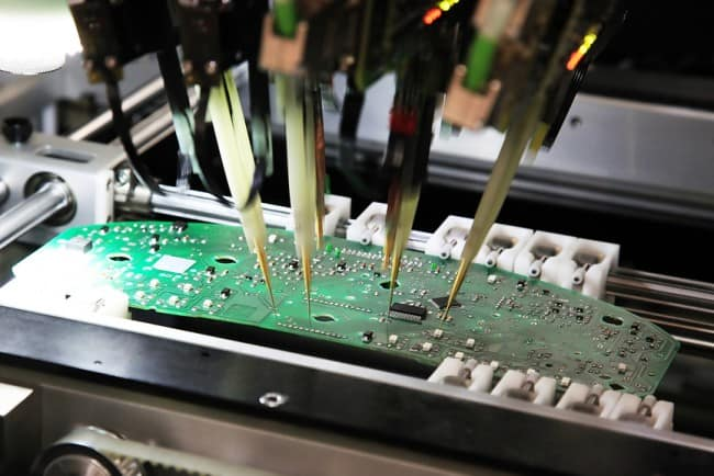
2. Assembly (PCBA): Following board fabrication, the PCB assembly (PCBA) stage involves mounting components onto the bare board through a soldering process. This step transforms the board into a functional electronic device.

PCB Testing: Ensuring Operational Functionality
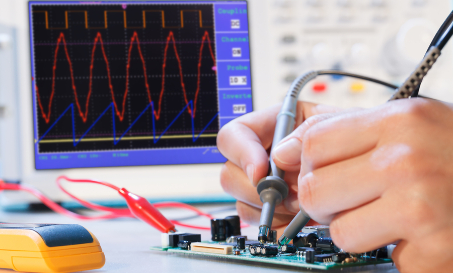
PCB testing, or bring-up, occurs after manufacturing to evaluate the board's operational functionality. Errors or areas for improvement are identified, initiating further design cycles. Testing during development is crucial for refining the design and enhancing overall performance.

Understanding the PCB Fabrication Process
The PCB fabrication process is the transformative journey from design to a physical structure based on design specifications. Key steps in this process include:
1. Imaging Layout on Copper Clad Laminates: Depicting the desired layout on laminates sets the foundation for the PCB.
2. Etching Inner and Surface Layers: Removing excess copper from inner and surface layers reveals traces and pads, refining the circuit.
3. PCB Layer Stackup Creation: Laminating board materials at high temperatures establishes the PCB layer stackup.
4. Drilling Holes: Holes for mounting, through-hole pins, and vias are drilled for component placement.
5. Plating Holes: Pin holes and via holes are plated to enhance conductivity.
6. Protective Coating: Applying a protective coating or solder mask safeguards the surface.
7. Silkscreen Printing: Printing reference indicators and markings on the surface aids assembly and maintenance.
8. Optional Finishing: Adding finishes to copper areas enhances surface properties.

The Significance of Understanding PCB Fabrication
The question arises: Is it crucial to understand the PCB fabrication process, considering it is an outsourced activity performed by a contract manufacturer (CM)? The emphatic answer is yes.
1. Manufacturability: Design choices impact manufacturability, including clearances, material selection, and considerations for panelization.
2. Yield Rate: Specifying parameters that stretch tolerance boundaries can result in a higher number of unusable boards.
3. Reliability: Meeting IPC-6011 classification ensures reliability, preventing inconsistent operation or premature failure.
Understanding the PCB fabrication process empowers designers to make informed choices, mitigating potential issues and optimizing the overall development, production, and operational phases.
Utilizing Design for Manufacturing (DFM)
To enhance the integration of fabrication knowledge into design decisions, the use of Design for Manufacturing (DFM) rules and guidelines is crucial. Employing comprehensive PCB design analysis tools, such as Cadence's Document Automation Tool, enables the creation of detailed views to aid CMs during the PCB fabrication process. This strategic approach safeguards against delays and additional manufacturing costs, ensuring a smoother and more efficient development journey.