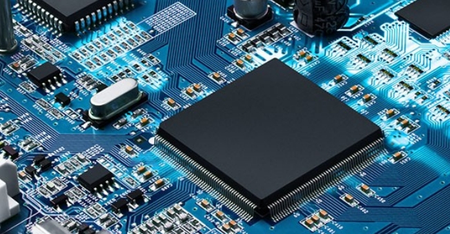
PCB (printed circuit board) is a key component of many electronic devices, such as computers, smartphones, TVs, and so on. PCBs are made of thin layers of copper and insulating materials, and they contain traces and pads that connect various components and circuits. PCB manufacturing and assembly are the processes of creating and assembling PCBs for different applications.

The PCB manufacturing process involves several steps, such as:
1.Design: The first step is to design the PCB layout using specialized software, such as CAD (computer-aided design). The layout specifies the size, shape, position, and connection of the components and traces on the PCB. The design also includes the number and type of layers, the thickness of the copper and the insulating material, and the drilling and soldering specifications.
2.Fabrication: The next step is to fabricate the PCB according to the design. The fabrication process involves:
3.Lamination: The copper and insulating layers are laminated together using heat and pressure. The number of layers depends on the complexity and functionality of the PCB.
4. Drilling: Holes are drilled through the layers to create vias, which are connections between different layers. The holes are also used to mount components on the PCB.
5.Etching: The unwanted copper is removed from the surface using a chemical solution, leaving only the desired traces and pads.
6.Plating: A thin layer of metal, such as tin or gold, is applied on the traces and pads to protect them from oxidation and corrosion.
7.Solder mask: A layer of green or other colored material is applied on the PCB to cover the traces and pads, except for the areas where components will be soldered. The solder mask prevents short circuits and improves the durability of the PCB.
8.Silkscreen: A layer of ink is printed on the PCB to label the components, symbols, logos, and other information. The silkscreen helps with identification and troubleshooting of the PCB.
9.Testing: The final step is to test the PCB for functionality and quality. The testing methods include:
10.Electrical testing: The PCB is checked for continuity, resistance, capacitance, voltage, current, and other electrical parameters using probes or fixtures.
11.Visual inspection: The PCB is examined for physical defects, such as cracks, scratches, misalignment, or solder bridges.
12. X-ray inspection: The PCB is scanned using X-rays to detect hidden defects, such as voids, shorts, or opens in the vias or solder joints.
The PCB assembly process involves attaching components to the PCB to form a functional electronic device. The components can be either through-hole or surface-mount. Through-hole components have leads that go through holes in the PCB and are soldered on the other side. Surface-mount components have terminals that are soldered directly on the pads on the surface of the PCB. The PCB assembly process includes:
1.Solder paste printing: A stencil is used to apply a thin layer of solder paste on the pads where surface-mount components will be placed. The solder paste contains tiny balls of metal that will melt and form solder joints when heated.
2.Pick-and-place: A machine picks up surface-mount components from reels or trays and places them on their corresponding pads on the PCB. The machine uses cameras or lasers to align the components accurately.
3.Reflow soldering: The PCB is heated in an oven to melt the solder paste and form permanent connections between the components and the pads. The temperature profile is carefully controlled to avoid overheating or underheating.
4.Through-hole soldering: For through-hole components, there are two methods of soldering:
5. Wave soldering: The PCB is passed over a wave of molten solder that wets the leads and forms solder joints.
6.Selective soldering: A robot applies solder selectively to specific areas where through-hole components are located.
7.Cleaning: The PCB is cleaned using water or solvents to remove any flux residue, dust, or contaminants that may affect its performance or reliability.
8.Inspection: The assembled PCB is inspected for defects, such as missing, misaligned, or damaged components, or poor solder quality. The inspection methods include:
9.Visual inspection: Human operators or machines use magnifiers or cameras to examine the assembled PCB.
10.Automated optical inspection (AOI): A machine uses cameras and software to compare images of the assembled PCB with a reference image and detect any anomalies.
11.Automated X-ray inspection (AXI): A machine uses X-rays to scan the assembled PCB and detect any hidden defects in the solder joints or vias.
12.Testing: The assembled PCB is tested for functionality and compatibility with other devices. The testing methods include:
13.In-circuit testing (ICT): A machine uses probes or fixtures to measure electrical parameters of individual components or circuits on the assembled PCB.
14.Functional testing (FCT): A machine or a human operator uses external equipment, such as power supplies, oscilloscopes, or multimeters, to simulate the operating conditions and verify the functionality of the assembled PCB.
15.System testing: The assembled PCB is integrated with other components or devices and tested as a whole system.
Conclusion
PCB manufacturing and assembly are complex and critical processes that require high precision, quality, and efficiency. By following the steps and methods described above, PCB manufacturers and assemblers can produce reliable and functional electronic devices for various applications.