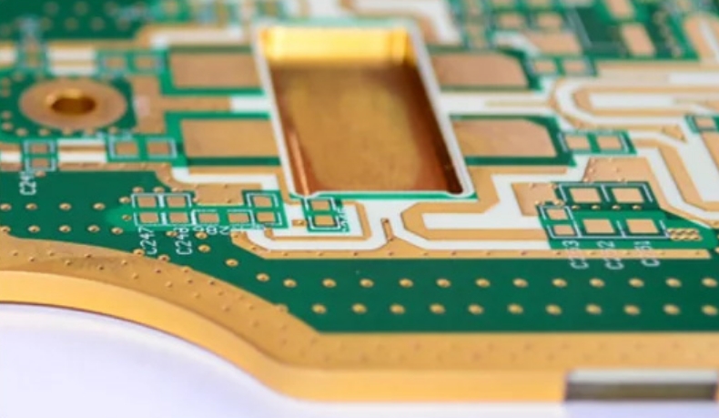
High Frequency PCB Design plays a crucial role in developing advanced electronic devices. Engineers can achieve superior performance in high frequency applications by optimizing the design of printed circuit boards (PCBs). This article will explore the fundamentals of High Frequency PCB Design, covering important concepts, considerations, and techniques that ensure reliable and efficient signal transmission.

To dive into the world of High Frequency PCB Design, it's vital to have a solid understanding of key concepts. High frequency circuits deal with signals that oscillate at higher frequencies, typically in the MHz (megahertz) or GHz (gigahertz) range. These circuits play a crucial role in various applications, including wireless communication, radar systems, and high-speed data processing.
In the realm of electronic signals, two fundamental types exist: analog and digital. Analog signals are continuous and represent real-world data, while digital signals are discrete and primarily consist of binary values (0s and 1s). High frequency circuits can work with both analog and digital signals, each requiring different approaches to PCB design.
When developing a high frequency PCB, several considerations must be taken into account to achieve optimal performance. One fundamental aspect is material selection. Choosing the appropriate materials with suitable dielectric properties and low loss tangents is crucial. It ensures minimal signal degradation, especially at higher frequencies.
Another important consideration is the use of ground planes. Ground planes act as a reference plane for signal return paths, reducing electromagnetic interference and improving signal integrity. By providing a solid conductive layer beneath the circuit traces, ground planes help create a clean and stable signal environment.
To further enhance signal quality, reducing crosstalk is imperative. Crosstalk occurs when signals from adjacent traces interfere with each other. By carefully routing traces and using proper spacing between them, crosstalk can be minimized, leading to improved overall circuit performance.
Optimizing component placement is a crucial design technique for high frequency PCBs. Placing components strategically can minimize the length of signal traces and reduce signal degradation or interference. It also enables efficient routing of crucial signals and improves overall signal transmission.
Signal transmission lines play a vital role in high frequency PCB design. These transmission lines, such as microstrips or striplines, are carefully designed paths used to transmit signals with controlled impedance. Matching the impedance of the transmission lines with the connected devices ensures efficient signal transfer and minimizes signal reflections.
Ensuring reliability is paramount in high frequency applications. High frequency PCBs may be subjected to harsh conditions, including temperature fluctuations and environmental factors. Therefore, selecting robust materials, implementing proper heat dissipation techniques, and considering the mechanical stability of the PCB are essential to guarantee reliable operation.
Designing high frequency PCBs comes with its own set of challenges. One significant challenge is signal reflections. When a signal encounters an impedance mismatch along its transmission path, a portion of the signal is reflected back, causing signal degradation. To mitigate this issue, designers must pay close attention to impedance matching techniques.
Another challenge lies in providing stable and clean power supplies for high frequency circuits. These circuits often require low noise and regulated power sources to maintain signal integrity. By implementing proper decoupling capacitors and well-designed power distribution networks, the stability and quality of power supply can be assured.
Increasing the spacing between adjacent signals is crucial in high frequency PCB design. As frequencies increase, electromagnetic fields around traces become more significant, leading to potential interference known as coupling. By ensuring adequate spacing and employing shielding techniques, designers can mitigate signal loss and interference.
Controlled impedance and differential pairing are advanced techniques used in high frequency PCB design. Controlled impedance refers to precisely maintaining a specified impedance value throughout the transmission lines, ensuring optimal signal transfer. Differential pairing involves transmitting signals using two conductors with opposite polarities to minimize noise and improve signal integrity.
For RF (Radio Frequency) and microwave applications, specific considerations must be made. These applications involve even higher frequencies, and thus, meticulous design techniques, shielding, and filtering are crucial. RF and microwave circuits require careful impedance matching and precise signal filtering to achieve optimal performance.
Understanding High Frequency PCB Design is essential for designing electronic systems that operate reliably at high frequencies. By considering material selection, proper grounding, reducing crosstalk, and optimizing component placement, engineers can ensure efficient signal transmission and maintain signal integrity. Overcoming challenges such as signal reflections, power supply stability, and interference is possible with careful design techniques. Advanced approaches like controlled impedance and differential pairing further enhance the performance of high frequency PCBs. With this knowledge, engineers can design robust and efficient electronic systems for a wide range of high frequency applications.
Q1. What are the key factors to consider in high frequency PCB material selection?
A1. The dielectric properties, loss tangents, and frequency range compatibility are crucial factors when selecting PCB materials for high frequency applications.
Q2. Why are ground planes important in high frequency PCB design?
A2. Ground planes help reduce electromagnetic interference, improve signal return paths, and enhance signal integrity in high frequency circuits.
Q3. How can crosstalk be minimized in high frequency PCBs?
A3. Crosstalk can be reduced by careful trace routing, maintaining proper spacing between traces, and utilizing shielding techniques.
Q4. Why is impedance matching crucial in high frequency PCB design?
A4. Impedance matching ensures efficient signal transfer by minimizing signal reflections and maximizing power transfer along transmission lines.
Q5. What are some common challenges in high frequency PCB design?
A5. Signal reflections, power supply stability, and managing interference are common challenges in high frequency PCB design.