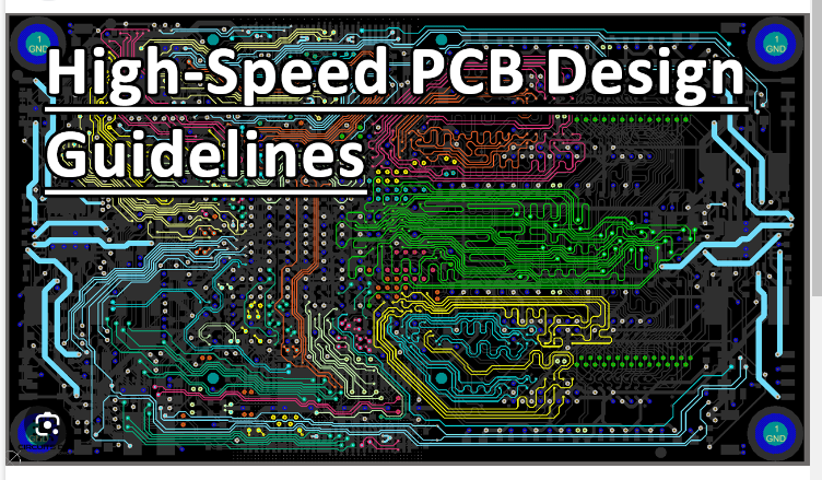
In today's fast-paced technological advancements, high-speed PCB design plays a crucial role in ensuring optimal performance for various electronic devices. A well-designed PCB layout can minimize signal integrity issues, reduce electromagnetic interference, and enhance the overall functionality of electronic circuits. In this article, we will delve into some essential guidelines that every PCB designer and engineer should consider when working on high-speed PCB designs.

In this digital era, almost every electronic device incorporates PCBs, also known as circuit boards. High-speed PCB design involves the layout and interconnections of various electronic components on a PCB to ensure the efficient operation of digital signals. It requires careful consideration of impedance, trace length, and signal integrity to achieve optimal performance.
Signal traces on a PCB act as conductive paths for transferring digital signals between different components. Impedance mismatches occur when the impedance of a trace changes abruptly, causing signal degradation and reflections. These can lead to timing issues and data corruption in high-speed circuits.
Maintaining signal integrity is vital for high-speed PCBs. Controlled impedance ensures the efficient transmission of signals without distortions or reflections. By carefully controlling the impedance of traces, designers can minimize signal degradation and maximize the performance of high-speed digital circuits.
In high-speed designs, trace length matching is essential for maintaining signal synchronization. Failure to match trace lengths can result in skew and timing errors. Proper trace length matching techniques, such as serpentine routing or delay adjustments, help ensure accurate data transmission across the PCB.
Transmission lines are vital components in high-speed PCB designs. To avoid signal degradation, it is crucial to consider their characteristic impedance, termination, and routing techniques. By following transmission line design best practices, designers can mitigate impedance variations and minimize signal reflections.
A clean return path is crucial for high-speed signal integrity. By providing a low impedance path for return currents, designers can prevent electromagnetic interference (EMI) and ground bounce. Proper placement of decoupling capacitors close to components and avoiding discontinuities in the return path are beneficial strategies.
Ground planes act as a reference for signal traces and provide a return path for currents. They play a vital role in reducing noise, crosstalk, and EMI. Proper allocation of ground planes, including the separation of analog and digital ground planes, helps isolate sensitive signals and enhances the overall performance of high-speed PCBs.
Power planes are employed to distribute power throughout the PCB. They play a crucial role in reducing voltage drops, minimizing noise, and ensuring adequate power delivery to components. Proper placement of power planes and appropriate decoupling techniques help maintain the desired voltage levels and minimize power-related issues.
High-speed routing involves careful planning and consideration to ensure signal integrity. One essential practice is maintaining appropriate spacing between signal traces to minimize crosstalk. Additionally, avoiding right-angle bends, using 45-degree or rounded traces, and reducing stub length are effective techniques for reducing signal degradation and reflections.
The PCB layout significantly affects the signal integrity of high-speed circuits. An optimized layout reduces transmission line losses, minimizes electromagnetic emissions, and helps prevent crosstalk. By applying the necessary guidelines and adhering to best practices, designers can achieve high-performance PCB layouts.
To ensure the success of high-speed PCB designs, several essential practices should be followed. These include minimizing crosstalk and EMI, carefully placing components to reduce noise, employing proper routing techniques, and implementing thermal management strategies.
Crosstalk and EMI are common challenges in high-speed PCB designs. By maintaining proper spacing between adjacent traces and considering ground plane placement, designers can minimize crosstalk and prevent signal interference. Shielding sensitive traces and employing filtering techniques can further reduce EMI.
Strategic component placement is critical to minimizing noise in high-speed PCBs. Keeping noisy components away from sensitive circuitry and ensuring proper ground connections are effective ways to reduce noise interference. By applying suitable decoupling techniques and segregating analog and digital components, designers can achieve better noise immunity.
Routing high-speed traces requires careful attention to signal integrity. Avoiding sharp bends, using wider traces, and reducing stubs are recommended practices for minimizing signal degradation. By routing high-speed signals away from noisy areas and crossing critical signals perpendicularly, designers can enhance signal quality.
High-speed circuits generate heat, which can impact performance and reliability. Effective thermal management techniques, such as using thermal vias, heatsinks, and sufficient copper pours, help dissipate heat and maintain optimal operating temperatures. Adequate cooling ensures the longevity and stability of high-speed PCB designs.
Conclusion
In the fast-paced world of electronics, high-speed PCB layout guidelines are paramount for optimizing signal integrity and minimizing performance issues. By adhering to best practices in circuit board design, impedance control, signal trace routing, and power distribution, designers can achieve efficient high-speed PCB layouts. By following these guidelines, a well-designed high-speed PCB contributes to the overall success of electronic products, delivering reliable performance and enhanced functionality.
What is the role of impedance mismatches in high-speed PCB design?
Impedance mismatches can lead to signal degradation, reflections, and timing issues in high-speed circuits.
Why is controlled impedance vital for signal integrity?
Controlled impedance ensures efficient transmission of signals, minimizing distortions and reflections.
How does trace length matching affect signal synchronization?
Trace length matching techniques prevent skew and timing errors, ensuring accurate data transmission.
What are the best practices for reducing crosstalk in high-speed PCBs?
Maintaining proper spacing between traces and careful ground plane placement help minimize crosstalk.
Which routing techniques are recommended for high-speed traces?
Avoiding sharp bends, using wider traces, and reducing stub length can minimize signal degradation.
These frequently asked questions provide further insight into high-speed PCB layout considerations and building successful high-speed PCB designs.