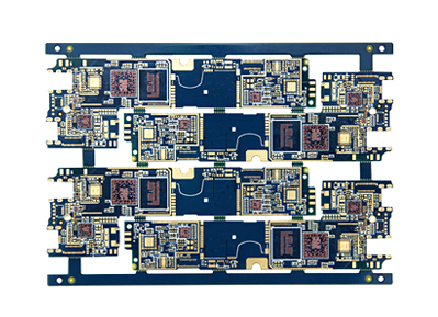
PCBs are used to connect electronic components together in a single board, allowing for easier assembly and troubleshooting. They consist of a flat board made of a non-conductive material (such as fiberglass) with copper traces and vias on one or both sides. The traces and vias provide a path for the electrical signals to flow between components, and the non-conductive material insulates the different traces from each other to prevent short circuits.

Standard PCBs are designed for less complex circuits and are typically constructed with fewer layers and larger conductive traces and vias. This means that they can support components with larger pitches and spaced farther apart. Standard PCBs are typically used in consumer electronics, toys, household appliances, and other applications that don't require high-density circuitry.
In contrast, HDI PCBs are designed for more complex circuits and are constructed with more layers and smaller conductive traces and vias. This allows for a higher density of components and interconnections, enabling them to pack more functionality into a smaller area. HDI PCBs use advanced manufacturing techniques such as laser drilling, sequential lamination, and microvias to create thinner and smaller vias and conductive traces, which allow for more complex and compact circuitry. HDI PCBs are commonly used in high-performance applications such as smartphones, tablets, and medical devices.
In summary, the main difference between HDI PCBs and standard PCBs is their construction and capabilities. HDI PCBs are designed for high-density, complex circuits with a greater number of layers and smaller conductive traces and vias, while standard PCBs are designed for less complex circuits with fewer layers and larger conductive traces and vias.
Get more knowledge about What is the difference between HDI and standard PCB please refer to Rigao PCB:https://www.rigaopcb.com