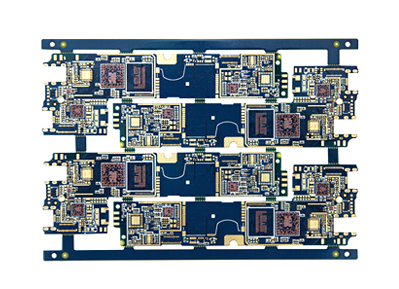
The High Density Interconnect (HDI) PCB manufacturing process is a specialized process used to create printed circuit boards (PCBs) that have a high density of components and traces. Here are the general steps involved in HDI PCB manufacturing:

1.Design: The first step is to design the PCB using Computer-Aided Design (CAD) software. This includes determining the board size, layer count, trace widths, hole sizes, and component placements.
2.Material selection: The next step is to select the appropriate materials for the PCB. This typically involves choosing the right substrate material (such as FR-4, polyimide, or ceramic) and copper foil thickness.
3.Drilling: In this step, holes are drilled in the substrate to create the vias and through-holes that will be used to connect the different layers of the PCB.
4.Plating: After drilling, the vias and through-holes are plated with copper to create electrical connections between the layers.
5.Imaging: A photoresist layer is applied to the surface of the copper, and a photomask is used to selectively expose the photoresist. The exposed photoresist is then developed, leaving behind a pattern that will be used to etch the copper.
6.Etching: The copper is etched away using an acidic solution, leaving behind the desired circuit pattern.
7.Lamination: In this step, the different layers of the PCB are laminated together using heat and pressure. This creates a solid board that is ready for component placement.
8.Component placement: Surface-mount components are placed on the board using automated pick-and-place machines. Through-hole components are manually inserted and soldered.
9.Soldering: The final step is to solder the components to the board using either wave soldering or reflow soldering.
Throughout the HDI PCB manufacturing process, quality control measures are taken to ensure that the board meets the necessary specifications and standards.
Get more knowledge about hdi pcb manufacturing process please refer to Rigao PCB:https://www.rigaopcb.com