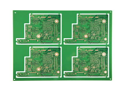
High-density interconnect (HDI) PCBs are advanced printed circuit boards (PCBs) designed to accommodate a high number of components and interconnections in a compact space. HDI PCBs are characterized by their fine lines and spaces, typically ranging from 50 to 100 microns, and their use of microvias to connect different layers of the board.

High Component Density: HDI PCBs can accommodate a large number of components in a small area, making them ideal for space-constrained applications.
Fine Lines and Spaces: HDI PCBs feature narrow conductive traces and small gaps between them, enabling the placement of more components on the board.
Microvias: Microvias are small-diameter vias that connect different layers of the HDI PCB, providing electrical connectivity while maintaining a compact board size.
Multilayer Construction: HDI PCBs are typically constructed with multiple layers, allowing for complex routing and signal integrity management.
Reduced Size and Weight: HDI PCBs are smaller and lighter than traditional PCBs, enabling the development of compact and portable electronic devices.
Improved Performance: HDI PCBs offer better electrical performance due to their controlled impedance and reduced signal loss.
Increased Reliability: The use of microvias and advanced materials in HDI PCBs enhances the board's reliability and durability.
Design Flexibility: HDI PCBs provide greater design flexibility, allowing for complex routing and the integration of various components.
Consumer Electronics: HDI PCBs are widely used in smartphones, tablets, laptops, and other portable devices.
Automotive Electronics: HDI PCBs are employed in automotive control modules, infotainment systems, and driver assistance systems.
Medical Devices: HDI PCBs are found in pacemakers, defibrillators, and other implantable medical devices.
Industrial Electronics: HDI PCBs are used in industrial controllers, sensors, and measurement equipment.
Aerospace and Defense: HDI PCBs are employed in satellites, missiles, and other military applications.
1.Minimum Trace and Space: HDI PCBs require small trace widths and spacing to achieve high circuit density. The minimum trace and space depend on the manufacturing capabilities of the PCB manufacturer, but typically range from 2 mils to 4 mils.
2.Via Size and Pitch: HDI PCBs use micro vias with small diameters (less than 0.2 mm) to connect multiple layers. The pitch between vias can be as small as 0.2 mm, and the aspect ratio of the vias should not exceed 1:1.
3.Pad and Annular Ring Size: The pad and annular ring sizes should be designed to accommodate the small via sizes used in HDI PCBs. Typically, the pad size is 2 to 3 times larger than the via size, and the annular ring size is at least 3 to 4 times larger than the via size.
4.Copper Weight: HDI PCBs require a thin layer of copper to achieve a high circuit density. The copper weight is typically 1 oz or less, and the plating thickness should be no more than 0.5 mils.
5.Tolerance and Inspection: HDI PCBs require strict tolerance and inspection standards to ensure that the PCBs meet the design specifications. The PCB manufacturer should use advanced inspection tools and techniques, such as X-ray inspection, to ensure the quality of the PCBs.
Overall, the HDI PCB design rules are critical to the successful fabrication and assembly of high-density PCBs. Designers should work closely with the PCB manufacturer to ensure that the design meets the manufacturer's capabilities and limitations.
HDI PCBs are sophisticated circuit boards that offer numerous advantages, including reduced size, improved performance, increased reliability, and design flexibility. Their applications span various industries, including consumer electronics, automotive, medical, industrial, and aerospace and defense. As technology continues to advance, HDI PCBs will play an increasingly critical role in enabling the development of smaller, more powerful, and more reliable electronic devices.
Get more knowledge about the hdi pcb design rules please refer to Rigao PCB:https://www.rigaopcb.com