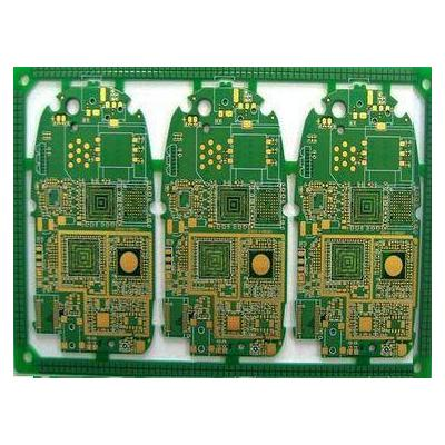
The fabrication process of HDI (High Density Interconnect) PCBs (Printed Circuit Boards) involves several steps, including design, material selection, drilling, plating, imaging, etching, lamination, and finishing. The process may vary slightly depending on the specific design requirements and the capabilities of the PCB manufacturer, but the following is a general overview of the HDI PCB fabrication process:

1.Design: The HDI PCB design process involves designing the circuit layout, choosing the appropriate materials and components, and determining the required features and specifications, such as minimum trace and space, via size and pitch, pad and annular ring size, and copper weight.
2.Material Selection: The PCB manufacturer selects the appropriate materials for the HDI PCB based on the design requirements, such as the substrate material, the copper foil, and the surface finish.
3.Drilling: The PCB manufacturer drills small-diameter holes, called micro vias, in the substrate material to connect the different layers of the PCB. The vias can be drilled using mechanical or laser drilling techniques, depending on the manufacturer's capabilities.
4.Plating: After drilling, the micro vias are plated with a thin layer of copper to form a conductive path between the layers. The plating process involves several steps, including cleaning, activation, deposition, and stripping.
5.Imaging and Etching: The PCB manufacturer applies a layer of photoresist to the surface of the PCB and exposes it to UV light through a photomask, which transfers the circuit pattern onto the photoresist. The PCB is then developed and etched to remove the unwanted copper and create the desired circuit pattern.
6.Lamination: The PCB manufacturer uses a lamination process to bond the layers of the PCB together, creating a multilayer structure. The layers are stacked, aligned, and pressed together under heat and pressure to form a solid and robust PCB.
7.Finishing: After lamination, the PCB is coated with a surface finish to protect the copper traces and pads from oxidation and corrosion. The surface finish can be a thin layer of gold, silver, or tin, depending on the design requirements.
Overall, the HDI PCB fabrication process is complex and requires advanced manufacturing techniques and equipment. The process is critical to the successful production of high-density and high-performance PCBs used in various electronic devices.
Get more knowledge about the hdi pcb fabrication process please refer to Rigao PCB:https://www.rigaopcb.com