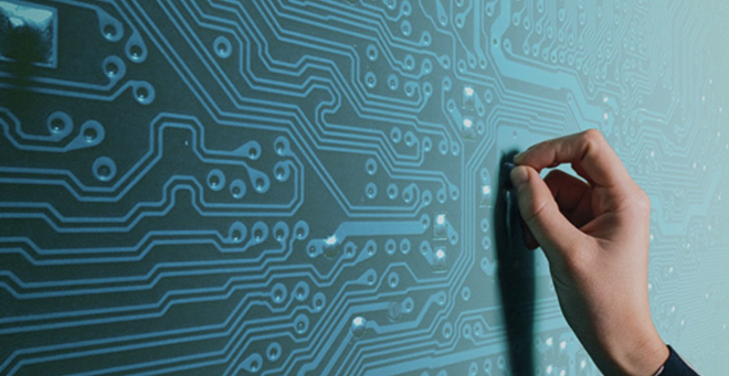
HDI technology is a method used in the manufacturing of printed circuit boards to create circuits with higher density and complexity. The main feature of HDI technology is the use of microvias, which are small holes drilled into the PCB that allow for the creation of more interconnections within a smaller surface area.

HDI technology can be used to create blind vias, which connect an outer layer of the PCB to an inner layer without penetrating the entire board, and buried vias, which connect two or more inner layers without penetrating the outer layers of the board. This enables the creation of more layers within a smaller surface area, resulting in a higher density of interconnects and more complex circuits.
HDI technology also enables the use of smaller trace widths and spacing, which allows for more efficient use of board space. This is particularly important for applications where size and weight are critical factors, such as mobile devices, aerospace, and medical equipment.
Overall, HDI technology enables the creation of smaller, more complex, and higher-performing circuits, which makes it well-suited for a wide range of applications that require high density and complexity in a small package.
Get more knowledge about what's hdi technology in pcb please refer to rigaopcb:https://www.rigaopcb.com/