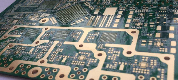
In PCB design, HDI (High Density Interconnect) refers to a technology that enables the creation of high-density and high-performance PCBs. The HDI technology uses microvias, blind vias, and buried vias to provide a dense and complex interconnect between the different layers of the PCB.

An HDI layer is a layer in the PCB that is specifically designed to support the HDI technology. The HDI layers are typically made up of thinner materials and are positioned between the inner layers of the PCB. They are used to provide interconnects between the different layers of the PCB using vias.
HDI layers are essential in creating PCBs that are smaller, lighter, and have higher functionality. They allow for the integration of more components in a smaller area, while also improving the overall electrical performance and reliability of the PCB.
The number and type of HDI layers required in a PCB design will depend on the specific requirements of the application, including the complexity of the circuit, the number of components, and the required electrical and thermal properties. The designer must carefully consider these factors and work with the PCB manufacturer to determine the best HDI layer configuration for their specific design.
Get more knowledge about What is HDI layer in PCB please refer to rigaopcb:https://www.rigaopcb.com/