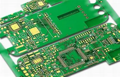
Designing HDI PCB can be challenging due to the small size of components, traces, and vias. Here are 8 tips to help achieve a successful HDI PCB design:

1.Start with a clear understanding of the design requirements: Before starting the HDI PCB design, it is important to have a clear understanding of the design requirements, such as the number and types of components, the signal speeds, and the thermal requirements. This will help in determining the layer stackup, the trace widths and spacing, and the via types that are required.
2.Use a PCB design software that supports HDI design: There are several PCB design software packages available that have advanced HDI design features, such as micro via support and layer stackup optimization. Using a software that supports HDI design will make the design process more efficient and help ensure that the design meets the required specifications.
3.Optimize the layer stackup: The layer stackup should be carefully optimized to ensure that the signal and power planes are properly separated to minimize noise and interference. This can include using multiple power planes and ground planes and placing signal layers between them.
4.Use the smallest possible vias: HDI PCBs use different types of vias, including blind vias, buried vias, and micro vias. Using the smallest possible via diameter and aspect ratio will help maximize the available routing area and reduce crosstalk and signal loss.
5.Place components carefully: Component placement is critical in HDI PCB design. Components should be placed in a way that maximizes the use of available space and minimizes signal interference. Decoupling capacitors should be located close to the power pins of the components they are intended to protect.
6.Optimize trace routing: Trace routing should be optimized to minimize the number of vias required and to ensure that high-speed signals have controlled impedance. Differential pairs should be routed together and with a consistent length and spacing to minimize crosstalk.
7.Use thermal management techniques: HDI PCBs have a higher density of components, which can lead to increased heat dissipation. Thermal management techniques, such as adding thermal vias, using copper pours, and optimizing component placement, should be employed to ensure that the PCB does not overheat and that the components are operating within their specified temperature ranges.
8.Collaborate with the manufacturer: Collaborating with the manufacturer throughout the design process can help ensure that the design can be manufactured cost-effectively and reliably. The manufacturer can provide feedback on the design and suggest modifications to optimize the manufacturing process.
Overall, achieving a successful HDI PCB design requires careful consideration of the layer stackup, via types, component placement, trace routing, thermal management, and collaboration with the manufacturer. With these tips in mind, an HDI PCB design can offer significant benefits in terms of miniaturization, higher density, improved signal quality, reduced cost, and increased reliability.
Get more knowledge about tips in Achieving Successful HDI PCB Design please refer to rigaopcb:https://www.rigaopcb.com/