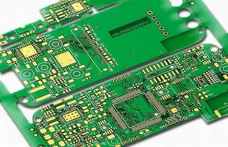
Are you new to HDI PCB? If so, you've come to the right place. In this beginner's guide, we will introduce you to the world of HDI PCBs. High-Density Interconnect PCBs, or HDI PCBs for short, are a type of printed circuit board that offer improved performance and miniaturization possibilities.

HDI PCBs have gained popularity in recent years due to the demand for smaller and more efficient electronic devices. They utilize advanced manufacturing techniques to achieve higher circuit densities, allowing more components to be integrated into a smaller area. This results in compact, lightweight, and technologically advanced devices.
What sets HDI PCBs apart from standard PCBs is their intricate design and construction. They employ microvias, which are tiny vias used to create connections between different PCB layers. By utilizing microvias, HDI PCBs effectively reduce signal distortion and improve signal integrity. This makes them ideal for high-speed and high-frequency applications.
There are several types of HDI PCBs available, including through-hole vias, blind vias, buried vias, and stacked vias. Each type offers its own advantages and is suitable for specific design requirements. Understanding the differences between these types is essential in choosing the right HDI PCB for your project.
In summary, if you're looking to design sleek and compact electronic devices with enhanced performance, HDI PCBs are worth considering. They provide the capability to integrate more components into a smaller space while maintaining signal integrity. Whether you're involved in the electronics industry or simply passionate about technology, delving into the world of HDI PCBs opens up exciting possibilities for innovation and advancement.