
Professional China PCB Assembly Online Services
 May 9, 2023
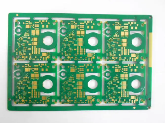
It is reliable and experienced in producing high-quality PCBs. A HDI PCB is a complex circuit board with multiple layers, high-density interconnections, and microvias, making it crucial to find a manu
Continue Reading....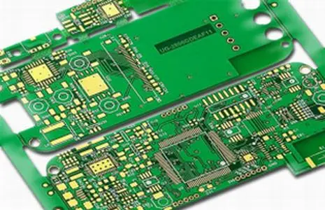 May 8, 2023
When choosing an HDI PCB manufacturer, there are a few key factors to consider:1.Experience: Look for a manufacturer with significant experience in producing HDI PCBs. This type of technology requires
Continue Reading....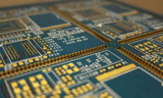 May 6, 2023
The HDI PCB market has seen significant growth in recent years, driven by the increasing demand for compact and high-performance electronic devices. Here is a brief analysis of the supply and demand f
Continue Reading.... May 5, 2023
Driven by the increasing demand for smaller, lighter, and more powerful electronic devices,HDI PCB technology has been evolving rapidly in recent years, Here are some trends and future developmen
Continue Reading....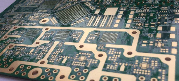 May 4, 2023
HDI PCBs are circuit boards that have a high density of electronic components and interconnections. HDI PCBs are designed with smaller vias and finer traces, allowing for more compact and efficient de
Continue Reading....
May 3, 2023
There are several important reasons in electronic manufacturing while using HDI PCB:1.Miniaturization: HDI PCBs allow for miniaturization of electronic devices. As technology adv
Continue Reading....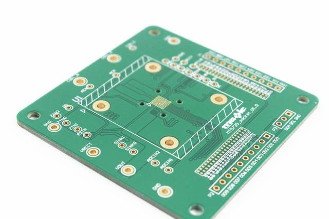 May 1, 2023
HDI stands for High Density Interconnect, which refers to a type of printed circuit board (PCB) technology that allows for higher circuit densities and finer trace widths than traditional PCBs. HDI PC
Continue Reading....
April 30, 2023
HDI PCB technology offers several benefits over traditional PCBs. Here are some of the key benefits of HDI PCB technology:1.Miniaturization: HDI PCBs can pack a higher density of components and interc
Continue Reading.... April 28, 2023
HDI PCBs are a type of printed circuit board that allows for a higher density of components and interconnections in a smaller footprint. Here are some crucial things to understand about HDI PCBs:1.Lay
Continue Reading....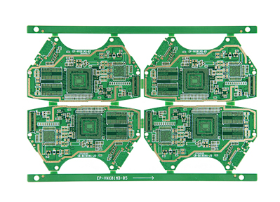 April 27, 2023
Designing HDI PCB can be challenging due to the small size of components, traces, and vias. Here are 8 tips to help achieve a successful HDI PCB design:1.Start with a clear understanding of the d
Continue Reading....
April 26, 2023
Choosing a PCB stackup is an important decision that depends on the specific requirements of the PCB design. Here are some factors to consider when selecting a PCB stackup:1.Number of layers: Determin
Continue Reading.... April 25, 2023
HDI PCB stackup is a type of printed circuit board design that allows for more components and connections to be packed into a smaller board area. This is achieved by using a combination of smaller via
Continue Reading....


