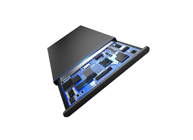
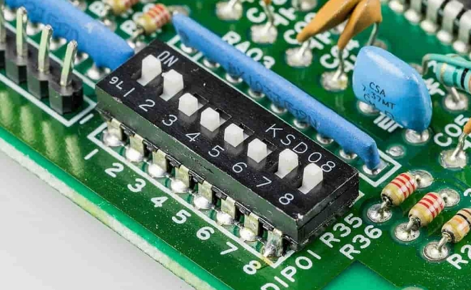
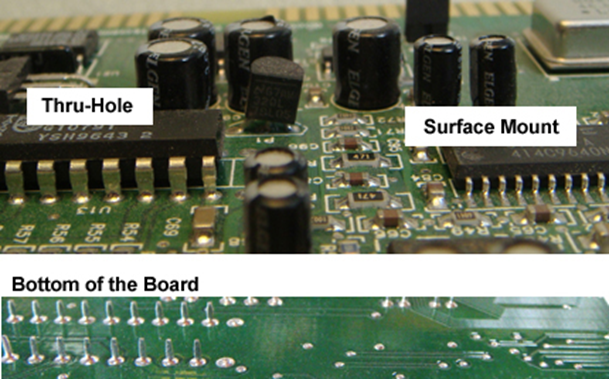
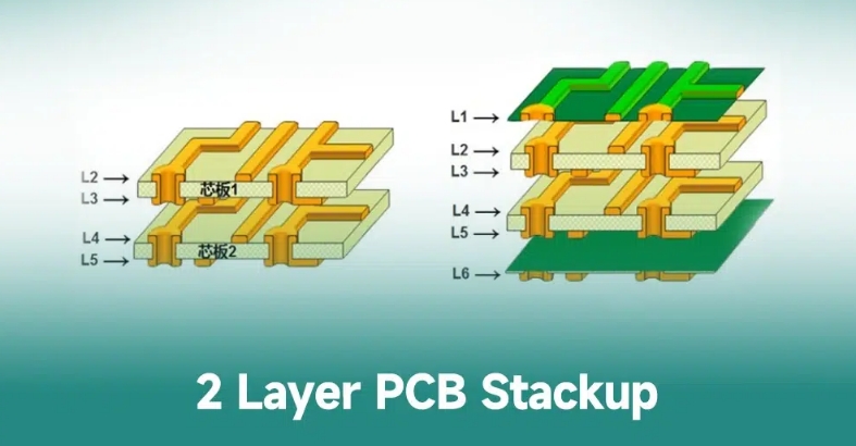
The advantages of Multilayer PCB include high assembly density, small volume and light weight. Due to high assembly density, the connection between components is reduced, so the reliability is improved. The number of wiring layers can be increased, thus increasing the flexibility of the design; Can form a circuit with a certain impedance; Can form a high-speed transmission circuit; The circuit and magnetic circuit shielding layer can be set, and the metal core heat dissipation layer can be set to meet the needs of shielding, heat dissipation and other special functions; Easy installation and high reliability. Multilayer PCB is the product of electronic technology developing to high speed, multi-function, large capacity and small volume.
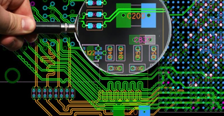
With the continuous development of electronic technology, especially the extensive and in-depth application of large-scale and ultra-large scale integrated circuits, multilayer pcb are rapidly developing to high density, high precision, high level digitalization direction. There have been micro-lines, small aperture through, blind holes & buried holes, embedded resistance, embedded capacity, impedance control, high plate thickness aperture ratio technology to meet the needs of the market.
Our Multilayer PCB process capacity is 40 layers, with impedance control and buried & blind holes requirements can also be met, and the inner and outer layer required with heavy copper thickness of 12oz can also be produced in Rigao Electronics, welcome to contact us at any time for your project.


